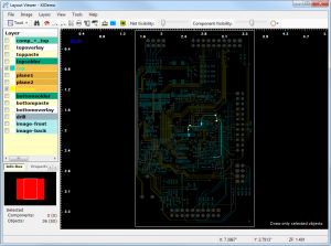
If your project uses an ODB++ netlist, then you can take advantage of the Layout Viewer in both XJDeveloper and XJRunner. Layout Viewer uses the layout information in the netlist to allow you to visualise the physical location of components, pins and nets on a board. This is especially useful for visualising errors from the connection test to guide you towards the most likely location of a fault on a board.
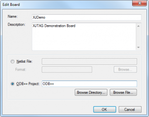
To use an ODB++ netlist, create or edit a board in XJDeveloper, and check the “ODB++ Project” radio button. Finally browse to the ODB++ file or directory and click OK.
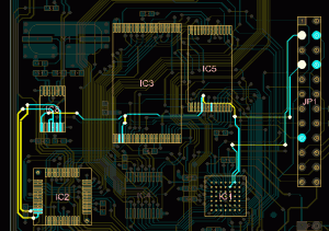
Once XJDeveloper has loaded the netlist, you will be able to view circuit elements in the viewer. This feature is available throughout XJDeveloper. For example you can right-click on a net and choose “Show in Layout Viewer”. The Layout Viewer will be opened and the net will be highlighted.
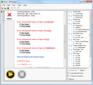
Errors in the connection test are displayed as hyperlinks (in both XJDeveloper and XJRunner). Clicking the links will display the nets in the Layout Viewer:
Future information on the Layout Viewer can be found in the help files.


Leave A Comment